Rapidus at the Halfway Mark: Why One Fab's Walls Became Japan's Industrial-Policy Test
In mid-September 2024, the shell of the IIM fab rising near New Chitose Airport in Chitose, on the northern island of Hokkaido, passed a threshold that few frontier semiconductor projects reach on schedule: more than 50% complete, with less than six months to go before the start of its cutting-edge semiconductor prototype line. The progress report, as Nikkei Asia reported, arrived wrapped in a number far larger than the building itself: a projected cumulative economic windfall of more than ¥18 trillion, about $120 billion, for the local and national economy of Japan through fiscal 2036. On the surface the story is simple — a factory is being built, and the country expects to grow rich from it. Read carefully, the story is a test: of whether the most ambitious industrial-policy bet Japan has placed in a generation can convert concrete into production, and of whether the windfall arithmetic survives contact with the parts of the project that are still promises rather than progress.
This article treats the halfway mark not as news but as evidence. A construction percentage is one of the few fully verifiable facts available about the Rapidus project at this stage; everything else on the timeline — 2-nanometer chip samples by July 2025, mass production in 2027 — is a target, and targets in advanced chipmaking have a history of moving. The analytical question is therefore twofold. First, why did the construction progress of a single fab become a regional industrial-policy test rather than a corporate building update? Second, what evidence, arriving in what order, would confirm the ¥18 trillion windfall thesis — and what evidence would break it?
The halfway mark: what "more than 50% complete" actually measures
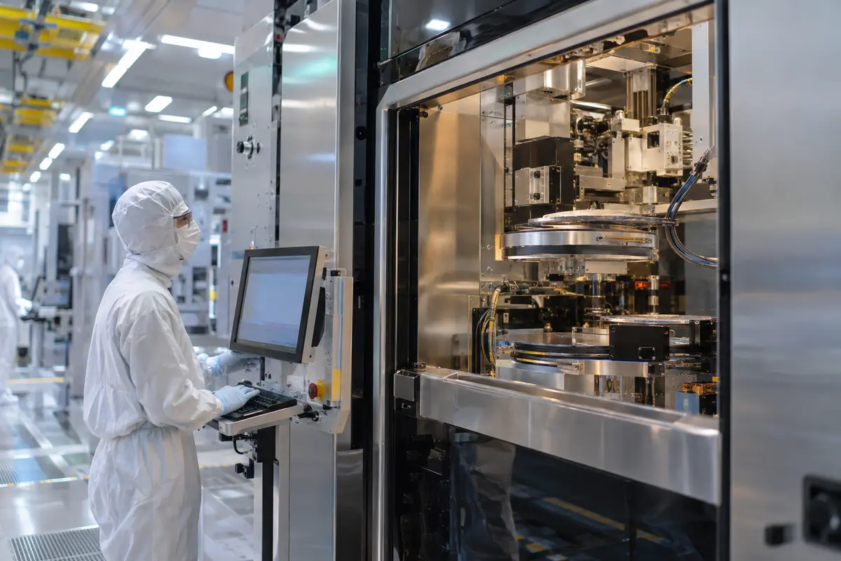
The IIM fab near New Chitose Airport is the physical centre of the attempt to return Japan to the frontier of logic chip manufacturing. As of mid-September 2024 the structure was more than 50% complete, and the prototype line — the first line, the learning line — stood less than six months from its start. Those two facts belong to different categories of evidence. A building that is half finished is half finished: poured concrete, erected steel and standing cranes are observable, countable and difficult to dispute in either direction. A prototype line described as "less than six months" from starting is a schedule claim, and schedules in advanced semiconductor manufacturing are precisely where optimism goes to be tested. The halfway mark therefore measures the completion of the container, not of the capability that must later live inside it.
- Construction: the IIM fab near New Chitose Airport in Chitose, Hokkaido, was more than 50% complete as of mid-September 2024;
- Prototype line: the cutting-edge semiconductor prototype line was less than six months from its start at that date;
- Samples: 2-nanometer chip samples are targeted by July 2025;
- Mass production: targeted for 2027;
- Cost: the total project cost is estimated at up to ¥5 trillion;
- Windfall: more than ¥18 trillion, about $120 billion, in projected cumulative local and national economic benefit through fiscal 2036.
Set side by side, the list shows a project whose verified half is construction and whose contested half is everything that happens inside the building afterwards. That asymmetry is the core of the doubts that accompany the coverage: hurdles to reaching mass production remain even while the structure rises on time. Nothing in the mid-September 2024 report contradicts the doubts, and nothing in the doubts contradicts the report; they describe different halves of the same project.
A milestone that carries policy weight
In most industries a half-finished plant is a corporate milestone. In advanced semiconductors it is a national one, because the capability being housed is among the scarcest on earth and the bill for housing it is among the largest: the total project cost is estimated at up to ¥5 trillion, which places the Chitose site among the biggest industrial bets in the country's recent history. When a project of that scale slips, the loss is not only a company's; it is the thesis that Japan can again host frontier logic manufacturing. A construction percentage thus reads as a policy indicator, because it is the earliest hard signal about whether that thesis is on time. The mid-September 2024 figure says the hard half is.
The ¥18 trillion promise: anatomy of a windfall thesis
The headline economics of the project are a projection: more than ¥18 trillion, roughly $120 billion, in cumulative local and national economic benefit through fiscal 2036. Three features of that number deserve unpacking before it is either celebrated or dismissed. It is cumulative rather than annual: spread across the years to fiscal 2036, it is a stream, and streams are sensitive to the date they begin, which is why every schedule slip in the project is also a subtraction from the promise. It is local and national at once: the windfall is claimed for Hokkaido and for Japan together, so the projection depends on effects — jobs, suppliers, spending, services — that radiate outward from the fab rather than staying inside its fence. And it is large relative to the cost: against a total project cost estimated at up to ¥5 trillion, a windfall of more than ¥18 trillion implies a return multiple of roughly three and a half times the entire bill, an assertion that the fab will generate value far beyond recouping its own construction.
None of this makes the number wrong. It makes it a thesis: a claim about a future production economy that does not yet exist, expressed in the language of present-tense benefit. The honest way to hold it is as a conditional — more than ¥18 trillion if the project reaches mass production and an ecosystem forms around it. The condition is the part that is not yet built, and it is the part the doubts in the coverage are about.
Land prices: the first effect already measurable
One component of the windfall story has already left the realm of projection: land. Hokkaido posted one of Japan's steepest land-price rises in 2024 — the third-highest among the country's regions — and the Rapidus effect is part of the explanation. Land prices are the economy's most forward-looking statistic: they price expectations of future income from a place, not current output from it. A third-place national ranking in land-price growth is therefore evidence that capital and households already believe some version of the windfall thesis strongly enough to pay for proximity to it, years before the first wafer earns a yen.
It is equally important to see what land prices cannot prove. They capture belief, not realisation. A land-price rise driven by an announced fab persists only if the fab is followed by the payrolls, suppliers and service economy the projection assumes; if mass production slips repeatedly, the same forward-looking mechanism works in reverse and unwinds the premium. The 2024 land-price data is thus best read as the first measurable vote of confidence in the thesis — and as the first indicator that would visibly crack if the thesis fails.
Why a single fab became a regional industrial-policy test
The concentration of the story in one building near one airport is not accidental. Advanced logic fabrication is among the most capital-intensive, skill-intensive and supplier-dependent manufacturing that exists; a single frontier fab anchors an ecosystem precisely because so much must co-locate around it, from equipment service to materials to trained process engineers. For Hokkaido, a region outside Japan's traditional manufacturing core, the Rapidus site is a rare chance to import that anchor rather than grow one over decades. For the national government, the fab is the visible edge of an attempt to re-enter frontier chipmaking. A regional development story and a national industrial-policy story therefore share a single coordinate: Chitose.
That fusion explains why construction progress carries the weight it does. If the project were merely a private investment, a halfway mark would be a balance-sheet event reported to shareholders. Because the project is also the test case for whether Japan can re-host frontier logic production, every verified milestone becomes public evidence about the policy itself, and every slip becomes an argument against it. The mid-September 2024 report — more than 50% complete, prototype line less than six months away — is, in that light, the first substantive verdict on the policy rather than on the building.
The equipment anchor: ASML's Chitose office
The ecosystem question has at least one concrete 2024 data point. ASML opened an office of about 25 people in Chitose in 2024, near the Rapidus site, to aid next-generation chipmakers including Rapidus and TSMC. Twenty-five people is a small headcount against a ¥5 trillion project, and it would be naive to read it as an ecosystem already formed. But supplier proximity in advanced lithography is not a courtesy: service, calibration and process support for cutting-edge tools depend on engineers being close to the fabs that run them. A vendor of ASML's role choosing to station staff in Chitose before the fab is even finished is a revealed-belief signal — the equipment side of the industry is positioning as if the Chitose project will need sustained on-site support, as if mass production is planned for rather than merely promised.
It is also a template for what confirmation would look like at the regional level: not announcements, but relocations. Offices, service depots, supplier plants and training programmes that move to Hokkaido because the fab exists are the windfall thesis becoming organisational fact, one lease and one payroll at a time. The ~25-person office is the first entry on that ledger.
The doubts: construction is not mass production
Against the verified half of the project stands the coverage's explicit caution: hurdles to reaching mass production remain despite the construction progress, as Nikkei Asia's coverage of the project underlines. The doubt is not about cranes. It is about the distance between a completed building and a yielding 2-nanometer line — a distance measured in tool installation, process integration, yield learning and talent, none of which are visible in a construction percentage. The stated sequence makes the gap concrete: a prototype line starting less than six months after mid-September 2024, 2-nanometer chip samples targeted by July 2025, and mass production targeted for 2027, all inside a project whose total cost is estimated at up to ¥5 trillion. Each step is a gate; each gate can slip; and the windfall projection assumes every gate opens on time.
- The prototype line's start. The first gate is calendrical: the line was less than six months from starting as of mid-September 2024. A start inside that window confirms that the verified half of the project transfers into the contested half; a slip reclassifies the halfway mark as the peak of the project's good news.
- 2-nanometer samples by July 2025. Samples are the first physical evidence that the process works outside simulation and documentation; their arrival on the stated target would be the strongest single confirmation available before mass production.
- Mass production in 2027. The windfall's production economy begins here; every year of slippage compresses the cumulative stream that is supposed to reach more than ¥18 trillion by fiscal 2036.
- Cost discipline against ¥5 trillion. The return multiple of the thesis — roughly three and a half times cost — shrinks directly with overruns, so a project that ends far above ¥5 trillion changes the arithmetic even in the success case.
- Ecosystem relocation in Hokkaido beyond announcements: supplier and service footprints, for which ASML's ~25-person Chitose office is the 2024 benchmark, plus the behaviour of the land-price signal that already turned positive in 2024 with the third-highest rise in the country.
What would break the thesis
The breaking scenarios are the mirror image of the confirming ones, and they are worth stating plainly, because a thesis that cannot be broken is not a thesis. A prototype line that starts late and a sample date of July 2025 that moves would not, by themselves, kill the windfall; they would reprice it, because cumulative projections are date-sensitive. A mass-production target that slides from 2027 into the back half of the decade would compress the stream toward fiscal 2036 and invite a downward revision of the ¥18 trillion figure itself. A cost estimate that climbs materially above ¥5 trillion would cut the return multiple even in the success case. And in Hokkaido the earliest visible break would likely be the signal the region already feels first: land prices that stop rising once the market concludes that the fab's payrolls and suppliers are not arriving. None of these had happened as of the mid-September 2024 report; all of them remain live, which is precisely why the coverage pairs a ¥120 billion windfall and open doubts in the same breath.
What to watch next
- The prototype line's start date measured against the six-month window that opened in mid-September 2024;
- July 2025: whether 2-nanometer chip samples are delivered on the stated target;
- The 2027 mass-production target and any revision to it;
- The ¥5 trillion total cost estimate and any upward movement in it;
- Successive land-price surveys for Hokkaido after its third-highest national rise in 2024, attributed in part to the Rapidus effect;
- The size and role of ASML's Chitose office beyond its initial ~25 people, and any further supplier relocations to the region;
- Any restatement of the more-than-¥18 trillion cumulative windfall projection through fiscal 2036.
The verdict of the halfway mark
The mid-September 2024 report gives Japan something rare in frontier chipmaking: a verified milestone. More than 50% of the IIM fab near New Chitose Airport was complete, with the prototype line less than six months from its start, in a project whose total cost is estimated at up to ¥5 trillion and whose promised return is more than ¥18 trillion cumulatively through fiscal 2036. The construction half of the story was, at that moment, on time; the production half remained a sequence of gates — samples by July 2025, mass production in 2027 — each of which the coverage honestly flags as uncertain.
That is why a single fab's walls became a regional industrial-policy test. Hokkaido's third-highest land-price rise in 2024 shows a region pricing the promise now; ASML's ~25-person office in Chitose shows the equipment industry positioning for the production; and the stated doubts mark the distance that remains between the two. The windfall thesis is neither confirmed nor broken at the halfway mark. It is, for the first time, testable — and the tests arrive in a known order: the prototype line, the samples, the mass production, the cost, and the land. A project that passes them will have earned its ¥18 trillion; a project that fails them will have demonstrated, expensively, that in semiconductors the hard half was never the concrete.






Leave a comment